STM32 microcontrollers are heavily used around the globe. The reason behind choosing stm32 MCU is numerous. The SDK is very stable. The Processors are ARM type and we do find a lot of examples and learning resources. In this post, I am going to explain the inner details of a popular STM32 board. STM32 mcu-based boards are branded as Nucleo Boards. They are quite extensible and easy to bring up.
Product Link: https://www.st.com/en/evaluation-tools/nucleo-f070rb.html
Microcontroller : STM32F070R8T6
It has Arduino UNO alike header as well
Product Overview
You can Go through the product overview document, Each Board has a corresponding board reference number. https://www.st.com/resource/en/data_brief/nucleo-f070rb.pdf
Hardware overview - UM1724
STMicroelectronics keep hardware reference guides and for our chosen board the User manual is UM1724
I would advise you to Go through this document https://www.st.com/content/ccc/resource/technical/document/user_manual/98/2e/fa/4b/e0/82/43/b7/DM00105823.pdf/files/DM00105823.pdf/jcr:content/translations/en.DM00105823.pdf
You can download the reference documents for future studies. Right now only going through this post will give you an overall idea of how to bring up this board and grasp enough tips/tricks to play around with it.
Take a close look at the board parts
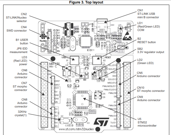
ST-LINK Programmer
STM MCU programmers are popularly known as ST-LINK. This board has an ST-LINK
The embedded ST-LINK/V2-1 supports only SWD for STM32 devices
New features supported on ST-LINK/V2-1:
- USB software re-enumeration
- Virtual COM port interface on USB
- Mass storage interface on USB
- USB power management request for more than 100 mA power on USB
Known limitation:
Activating the readout protection on ST-LINK/V2-1 target prevents the target application from running afterward. So during development, The target readout protection must be kept disabled on ST-LINK/V2-1 boards.
ST-Link options
Power Supply options
If your stm32 and additional shield require more than 300mA current then choose any of the external options
USB power options
If you choose option 1 above then you can see there are 2 modes one is 100mA another one is 300mA, you can select this by JP1 jumper

300mA will flow if
The host can provide up to 300mA
The host has USB enumeration support: i.e. host can detect USB device
JP1 is Off
Then, at first, the host will provide 100mA, during USB enumeration 300mA will flow as it is needed at that time.
In another case when JP1 is off & a USB charger is used to power the board through CN1 then the following happens
ST-Link gets powered up, 100mA flows
USB enumeration is absent at host [charge] but 300mA is required
as the charger does not have USB enumeration so stm32 is not powered
In this case, JP1 should be on to power stm32 anyway
We will keep JP1 off & use the U5V internal option
LD3 PWR the red led indicates that the stm32 part is powered and +5V power is available
JP6(IDD) should be on, an ammeter may be connected to it in series if you want to measure the current draw by the stm32
Vdd = 2.4V to 3.6V
VddA = from Vdd to 3.6V [external analog power supply for ADC]
POR = power on reset
At startup, It monitors Vdd voltage
the device remains in reset mode if Vdd is below 2V
VDDA should arrive first and must be greater than or equal to VDD , VDDA powers up the clock, and Power supply supervision blocks
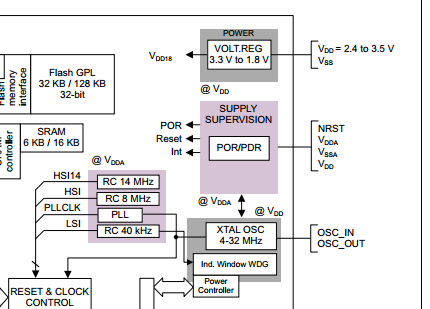
PDR = power down reset
It monitors both Vdd & VddA voltage
the device remains in reset mode if Vdd or VddA is below 2V
Max CPU Freq = 48MHz
3 low power modes
Clock

System clock selection is performed on the startup
On reset, the internal RC 8 MHz = HSI is selected as the default CPU clock
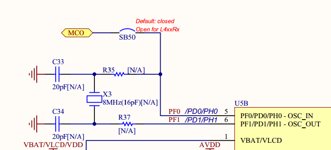
Ideally, a crystal oscillator is connected to OSC_IN, OSC_OUT pins pair and the PLL multiplies the crystal oscillator signal to PLLCLK which becomes the CPU clock
For example, a production circuit has the following setup where A fixed 16MHz crystal oscillator is connected to OSC_IN and OSC_OUT
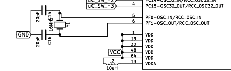
MCO: STM32 has the possibility to bring out a clock signal on a PIN called `MCO`. It takes one of the selected clock sources, puts it through a divider, and brings it out to a GPIO pin
The Nucleo board which I am using is MB1136 C-03, by default in this board the MCO output from ST-Link is used as the input clock to OSC_IN [ PF0, PF1 ]. it is fixed at 8MHz, you can see it in the following picture.
do not get confused by X3 as shown here. It is not present in MB1136-C03 [N/A is shown ]
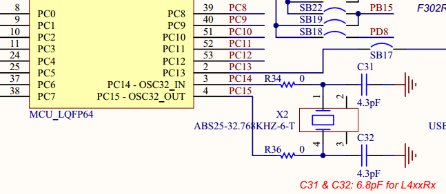
RTC-Clock
The MCU has internal RTC clock, it’s sources can be
A 32.768 kHz external crystal
Internal low-power RC oscillator [ 40KHz ]
High-speed external clock [ divided by 32 ]
A resonator or oscillator
By default, The MB1136 C-03 board has an onboard ABS25 crystal oscillator [ 32.768 KHz] as the clock source for the RTC. The crystal is connected to the OSC32_IN OSC32_OUT [ pin PC14, PC15 ]
USART
The MCU has upto 4 USART
The pins corresponding to USART2 are PA2 and PA3

In the MB1136 C-03 board by default, these pins are connected to ST-Link MCU ( STLK TX, STLK RX) near the CN3 connector

Jumper states [ default ]
The TX, RX at CN3 becomes a virtual COM port for the mBed platform
In Next Post we will Setup IDE and Toolchain to Program the microcontroller


very Interesting and knowledgeable articles posted by the author
ReplyDeleteJTAG